

 Product
 Brand
Brand Articles
 Tools
Tools
LDO vs Buck Converter: Which Power Regulator Is Best For Your Application?
Quick answer
An LDO is usually the simpler choice when the input is only slightly above the required output, the calculated heat is acceptable, and low output noise or low electromagnetic interference is important. A buck converter is usually the stronger choice when the voltage reduction or load current would make a linear regulator waste too much power.
Do not choose between them from a fixed voltage-gap or current threshold. Calculate the worst-case input range, load profile, regulator loss, junction temperature, battery runtime, noise requirement, and available PCB area. If the source can fall both above and below the required output, neither a basic LDO nor a buck converter can regulate across the full range; a buck-boost topology may be required.
What Is an LDO?
A low-dropout regulator, or LDO, is a linear regulator designed to maintain regulation with a relatively small difference between input and output voltage. Its control loop compares a feedback signal with a reference and adjusts a series pass device so that the output remains regulated.
The pass device operates as a controlled linear element. It does not convert the unused voltage into another form of useful energy: most of the electrical power represented by the input-to-output voltage difference and load current becomes heat in the regulator. The exact pass-device architecture, dropout behavior, ground current, stability requirements, and protection functions depend on the selected device.
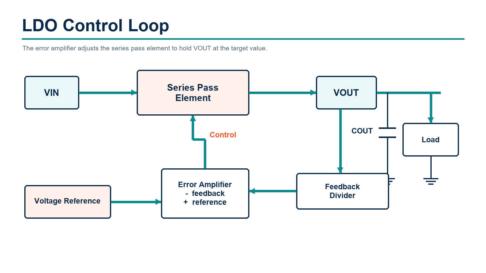
A simplified LDO feedback loop. The error amplifier controls the series pass element from the voltage reference and divided output feedback.
Dropout voltage is not a universal LDO value. It changes with output current, temperature, process variation, package, and architecture. The relevant check is the maximum specified dropout under the worst operating conditions, plus margin for input tolerance and transients.
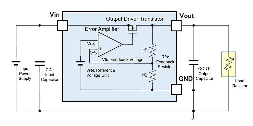
Original manufacturer illustration retained from the legacy article. Source: Nisshinbo Micro Devices.
Where an LDO is attractive
Low-noise analog, data-converter, RF, clock, or sensor rails.
Small input-to-output voltage differences with acceptable dissipation.
Low component count and simple layout.
Post-regulation after a switching converter.
Always-on rails where the chosen LDO has suitable quiescent and shutdown current.
What must be checked
Maximum dropout voltage at the required load and temperature.
Power dissipation and junction temperature on the actual PCB.
Required input and output capacitance, capacitor type, and effective capacitance after DC-bias derating.
Output noise and power-supply rejection ratio at the frequencies that matter.
Minimum load, reverse-current behavior, startup, enable, current limit, and thermal protection.
What Is a Buck Converter?
A buck converter is a switching DC-to-DC topology that steps a higher input voltage down to a lower regulated output. A controller rapidly switches the power stage, while an inductor and capacitors store and transfer energy. Synchronous buck regulators use a controlled low-side MOSFET; nonsynchronous designs normally use a diode for the low-side current path.
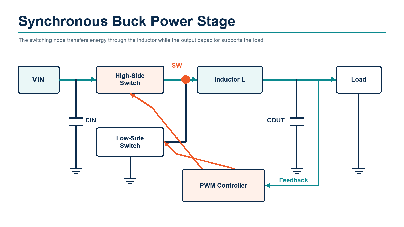
A simplified synchronous buck power stage. The input capacitor, switching node, inductor and output capacitor form the main energy-transfer path.
For an ideal buck converter operating in continuous conduction, the first-order relationship is VOUT = D x VIN, where D is duty cycle. A real design must include conduction loss, switching loss, dead time, minimum on-time, minimum off-time, inductor ripple, current limit, and control-mode behavior.
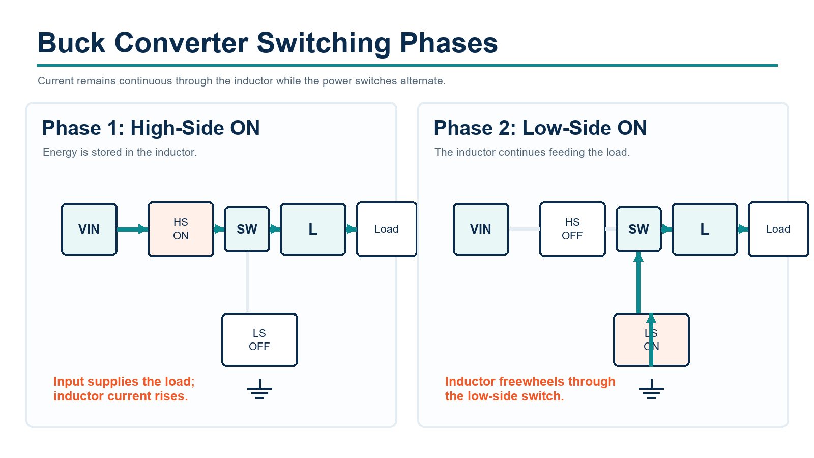
The two principal switching intervals in a synchronous buck converter. Inductor current continues feeding the load in both phases.
A buck converter can be far more efficient than an LDO when the voltage reduction or load current is large, but efficiency is never a fixed property of the topology. Use the selected regulator's efficiency curves or a loss model at the actual input voltage, output voltage, switching frequency, and load current. Light-load operating mode and quiescent current can dominate battery performance when average load is low.
Where a buck converter is attractive
Large input-to-output voltage ratios.
Moderate or high load current where LDO heat would be excessive.
Battery-powered systems where conversion efficiency materially affects runtime.
Power rails that need high power density or lower thermal loss.
What must be checked
Full input range, output voltage, continuous load, transient load, and peak inductor current.
Minimum on-time, minimum off-time, current limit, startup, and duty-cycle constraints.
Inductor value, saturation current, current ripple, core loss, and temperature rise.
Input and output capacitor ripple current, effective capacitance, ESR, and voltage rating.
Switching frequency, control mode, light-load behavior, output ripple, audible-noise risk, and EMI.
PCB layout. The high di/dt input loop and switch-node area must be kept small.
LDO vs. Buck Converter Comparison
| Decision factor | LDO | Buck converter |
|---|---|---|
| Conversion method | Linear pass element | Switched energy transfer |
| Ideal use | Small voltage drop and acceptable heat | Large voltage drop or higher power |
| Efficiency | Primarily limited by output-to-input voltage ratio and ground current | Depends on operating point, losses, frequency, and control mode |
| Output noise | No switching node; device noise and input-ripple rejection still matter | Switching ripple and high-frequency edges require filtering and layout control |
| Thermal behavior | Loss rises directly with voltage drop and load current | Often lower loss, but MOSFET, inductor, and IC temperatures must be checked |
| External parts | Usually input and output capacitors | Usually an inductor plus input and output capacitors; some designs need more parts |
| Layout sensitivity | Moderate; grounding and capacitor placement still affect performance | High; power-loop geometry directly affects ripple, ringing, and EMI |
| Step-up capability | No | No |
These are topology-level tendencies, not guaranteed device specifications. A low-IQ buck can outperform an LDO at light load, while a carefully selected LDO can be more efficient than a poorly matched buck when the voltage difference is small. Compare real parts at the real operating points.
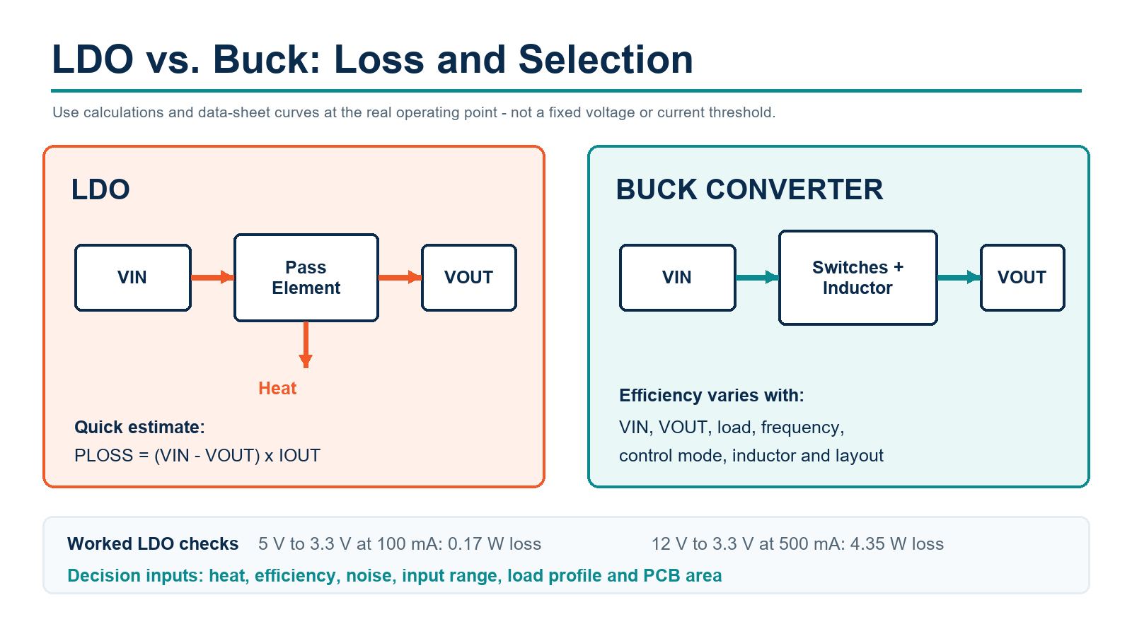
LDO loss can be screened directly from voltage drop and load current. Buck efficiency must be checked from the selected device at the actual operating point.
Efficiency and Thermal Calculations
LDO efficiency
The general efficiency expression is:
Efficiency = (VOUT x IOUT) / (VIN x IIN) x 100%
When LDO ground current is very small compared with load current, input current is approximately equal to output current and the quick estimate becomes:
Efficiency approximately equals VOUT / VIN x 100%
This approximation is not reliable at very light load or for regulators whose ground current is not negligible.
LDO power loss
A useful estimate that includes ground current is:
PD = (VIN - VOUT) x IOUT + VIN x IGND
Use maximum input voltage, realistic worst-case load, and the data-sheet ground-current value that applies to the operating condition. Startup, current limit, dropout, and reverse-current events may require separate analysis.
First-pass junction-temperature estimate
TJ approximately equals TA + PD x thetaJA
This equation is a screening calculation, not a substitute for board-level thermal validation. Published thetaJA values depend on a standardized test board and can differ substantially from the finished PCB. Package copper, thermal vias, airflow, nearby heat sources, and enclosure temperature all matter.
Buck-converter efficiency
For a buck converter, use the data-sheet efficiency curve or loss model at the intended operating point:
PLOSS = PIN - POUT
Efficiency = POUT / PIN x 100%
Conduction, switching, gate-drive, control, inductor, capacitor, and board losses all contribute. A single headline efficiency number cannot describe performance across the full load range.
How to Choose Between an LDO and a Buck Converter
Define the complete input range.
Include source tolerance, battery charge and discharge limits, adapter variation, startup behavior, and transients. Confirm whether the source always remains above the required output by enough headroom.
Define the load profile.
Record sleep, idle, typical, peak, and transient current. Average current affects battery runtime; peak current and slew rate affect regulation and component sizing.
Calculate LDO loss before rejecting or accepting it.
Use worst-case input voltage and load. Estimate junction temperature on the intended board. If the resulting temperature or efficiency is unacceptable, move to a switching solution.
Check light-load behavior.
For always-on battery rails, compare LDO ground current with buck operating current and shutdown current. Also check whether a buck enters pulse-skipping or burst operation and whether that behavior is acceptable.
Translate "low noise" into measurable limits.
Specify output-noise bandwidth, allowable ripple, sensitive frequencies, and required PSRR at those frequencies. LDO output noise and PSRR are separate specifications, and PSRR normally varies strongly with frequency, headroom, load, and capacitor selection.
Check physical implementation.
An LDO may use fewer components, but its copper area can grow when heat must be spread. A high-frequency buck may use smaller passives, but routing, switch-node placement, and EMI filtering can dominate the layout.
Validate the complete data sheet.
Confirm absolute maximum ratings, recommended operating conditions, accuracy over temperature, current limit, startup, stability, component derating, protection behavior, and package thermal data. Do not select a regulator from nominal voltage and current alone.
Worked Selection Examples
Example 1: 5 V to 3.3 V at 100 mA
An LDO's approximate conversion efficiency is 3.3 / 5 = 66%. Ignoring ground current, its dissipation is (5 - 3.3) x 0.1 = 0.17 W. That may be thermally acceptable in many packages and boards, but the decision still depends on ambient temperature, package thermal performance, battery-life target, and noise requirements. A buck can improve conversion efficiency, but it adds switching behavior and an inductor.
Example 2: 12 V to 3.3 V at 500 mA
An LDO would dissipate approximately (12 - 3.3) x 0.5 = 4.35 W before adding ground-current loss. That is normally an impractical thermal burden for a small linear regulator. A buck converter is the natural starting point, followed by an LDO only if a sensitive sub-rail needs additional noise reduction and the post-regulator has sufficient headroom.
Example 3: One lithium-ion cell to a regulated 3.3 V rail
A cell may begin near 4.2 V and later fall close to or below 3.3 V. A 3.3 V LDO regulates only while the battery remains above 3.3 V plus the required headroom. A buck converter also cannot maintain 3.3 V once its input is too low. If the system must hold 3.3 V across the full battery range, evaluate a buck-boost converter. If the load tolerates a falling rail, an LDO may still be appropriate, but that must be an explicit system decision.
Example 4: Low-noise analog rail from a 12 V input
A common architecture is a buck converter that creates an efficient intermediate rail, followed by a low-noise LDO. Set the buck output high enough to preserve the LDO's worst-case headroom, including ripple and transients, but not so high that the LDO wastes unnecessary power. Check LDO PSRR at the buck switching frequency and its harmonics; a strong low-frequency PSRR number alone is not enough.
Device Examples and What They Illustrate
The parts below illustrate different design priorities. They are not drop-in substitutes for one another and are not universal recommendations. Verify the latest data sheet, package, orderable suffix, lifecycle status, and availability before design-in.
Texas Instruments TPS7A02
The TPS7A02 is an active 200 mA fixed-output LDO family with a typical quiescent current of 25 nA. TI specifies a 1.5 V to 6 V input range and a maximum dropout of 270 mV at 200 mA for the 3.3 V version. It is an example of an LDO optimized for always-on and battery-sensitive loads, but its noise, dropout, package, and transient behavior still need to match the application.
Analog Devices LT3080
The LT3080 is a 1.1 A adjustable linear regulator that Analog Devices marks as recommended for new designs. It offers output adjustment down to 0 V, a wide input range, and a specified 350 mV dropout for packages other than SOT-223 under the stated data-sheet conditions. It is useful when adjustability and current capability matter, but a high input-to-output voltage difference can still create substantial heat.
Texas Instruments LM2596
The LM2596 is an active 150 kHz, 3 A buck-regulator family with a 4.5 V to 40 V input range. It illustrates a low-frequency, externally compensated-by-design SIMPLE SWITCHER approach that uses an external inductor and diode. Use the exact fixed or adjustable version's data sheet and design equations; the 3 A rating does not mean every layout or operating condition can deliver 3 A without thermal and current-limit checks.
View LM2596S-5.0/NOPB at Utmel
Analog Devices LTC3605
The LTC3605 is a production-status 5 A synchronous buck regulator with a 4 V to 15 V input range and an adjustable 800 kHz to 4 MHz switching frequency. Analog Devices specifies efficiency up to 96% under selected conditions. It illustrates how an integrated synchronous power stage and high switching frequency can support compact, high-current rails, while making layout and thermal design especially important.
Frequently Asked Questions
Can an LDO ever be more efficient than a buck converter?
Yes. When the input voltage is close to the output voltage and load current is low, the LDO's loss can be smaller than a buck converter's switching, control, and quiescent losses. Compare actual devices at the actual load profile instead of assuming one topology always wins.
Does an LDO remove all buck-converter noise?
No. An LDO attenuates input ripple according to its PSRR, which varies with frequency, headroom, load, and capacitor network. High-frequency switching components may pass through the LDO or couple around it through the PCB. Filtering and layout remain necessary.
Can a buck converter regulate when input voltage falls below output voltage?
No. A basic buck converter only steps voltage down. When the input range crosses the required output, use a topology that can both step down and step up, such as a suitable buck-boost converter.
Is a higher switching frequency always better?
No. Higher frequency can reduce inductor and capacitor size, but it often increases switching loss and may complicate EMI and thermal performance. Select frequency as part of a complete efficiency, size, noise, and input-range tradeoff.
What is the most important LDO thermal check?
Calculate worst-case power dissipation and estimate junction temperature using the package and board conditions. Then verify with the data sheet and, for thermally significant designs, board measurement. Do not rely on current rating alone.
What is the most important buck-layout rule?
Follow the manufacturer's reference layout and keep the high di/dt input current loop small. Place the input bypass capacitor close to the converter's power input and return pins, and minimize the switch-node area while meeting thermal requirements.
When should I use a buck converter followed by an LDO?
Use the combination when a large voltage reduction makes a linear-only solution inefficient but a sensitive load still benefits from lower ripple or noise. Budget enough LDO headroom at the worst case and verify PSRR at the converter's switching frequencies.
Conclusion
The practical choice is driven by quantified loss, heat, noise, input range, and load behavior. Choose an LDO when its simplicity and low switching noise are valuable and its calculated dissipation is acceptable. Choose a buck converter when a linear solution would waste too much power. Choose buck-boost when the input crosses the target output, and consider a buck-plus-LDO architecture when efficiency and low-noise regulation are both required.
The final decision belongs to the exact device and PCB, not the topology name. Use worst-case data-sheet limits, component derating, layout guidance, and hardware measurements before release.
Engineering References
Texas Instruments: LDO Basics design guide
Analog Devices: How to Successfully Apply Low-Dropout Regulators
Analog Devices AN-140: Basic Concepts of Linear Regulator and Switching Mode Power Supplies
Texas Instruments SLVA477B: Basic Calculation of a Buck Converter's Power Stage
Texas Instruments: Buck-regulator layout and EMI considerations
 UTMEL
UTMEL
We are the professional distributor of electronic components, providing a large variety of products to save you a lot of time, effort, and cost with our efficient self-customized service. careful order preparation fast delivery service
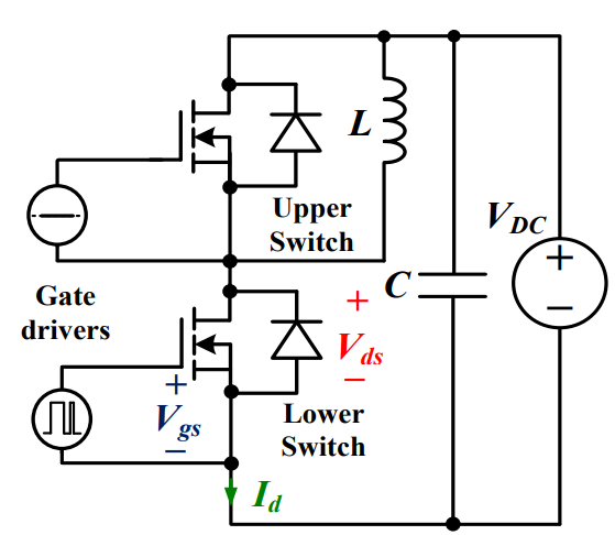 Discovering New and Advanced Methodology for Determining the Dynamic Characterization of Wide Bandgap DevicesSaumitra Jagdale15 March 20242873
For a long era, silicon has stood out as the primary material for fabricating electronic devices due to its affordability, moderate efficiency, and performance capabilities. Despite its widespread use, silicon faces several limitations that render it unsuitable for applications involving high power and elevated temperatures. As technological advancements continue and the industry demands enhanced efficiency from devices, these limitations become increasingly vivid. In the quest for electronic devices that are more potent, efficient, and compact, wide bandgap materials are emerging as a dominant player. Their superiority over silicon in crucial aspects such as efficiency, higher junction temperatures, power density, thinner drift regions, and faster switching speeds positions them as the preferred materials for the future of power electronics.
Read More Applications of FPGAs in Artificial Intelligence: A Comprehensive GuideUTMEL29 August 20255561
This comprehensive guide explores FPGAs as powerful AI accelerators that offer distinct advantages over traditional GPUs and CPUs. FPGAs provide reconfigurable hardware that can be customized for specific AI workloads, delivering superior energy efficiency, ultra-low latency, and deterministic performance—particularly valuable for edge AI applications. While GPUs excel at parallel processing for training, FPGAs shine in inference tasks through their adaptability and power optimization. The document covers practical implementation challenges, including development complexity and resource constraints, while highlighting solutions like High-Level Synthesis tools and vendor-specific AI development suites from Intel and AMD/Xilinx. Real-world applications span telecommunications, healthcare, autonomous vehicles, and financial services, demonstrating FPGAs' versatility in mission-critical systems requiring real-time processing and minimal power consumption.
Read More The 2026 Engineer’s Guide: Choosing the Right MCU for Your Next IoT & New Energy ProjectUTMEL30 April 20261817
A comprehensive comparison of 2026's leading MCUs from ST, NXP, and Microchip across power efficiency, processing performance, connectivity, and ecosystems to help engineers select the optimal chip for next-gen IoT and new energy projects.
Read More AI Server Components: Engineering Next-Gen Data Center Hardware for 100kW RacksUTMEL15 May 2026991
The transition from traditional enterprise IT to AI-driven workloads has rendered legacy data center hardware obsolete, forcing infrastructure planners to re-engineer server components for extreme thermal environments.
Read More The Practical Engineer’s Guide to the NE555N Timer: Pinout, Setup, and TroubleshootingUTMEL29 May 2026783
This comprehensive guide explores the NE555N timer, detailing its 8-pin layout, internal architecture, and key datasheet specifications. It compares the bipolar IC to CMOS variants and details setup configurations for astable, monostable, and bistable modes. Additionally, the guide offers practical troubleshooting advice to prevent common breadboard failures, such as floating reset pins and electrical noise issues.
Read More
Subscribe to Utmel !
![ADUM4223BRWZ]() ADUM4223BRWZ
ADUM4223BRWZAnalog Devices Inc.
![ADUM3221ARZ]() ADUM3221ARZ
ADUM3221ARZAnalog Devices Inc.
![HCS301/SN]() HCS301/SN
HCS301/SNMicrochip Technology
![AT88SC0808CA-Y6H-T]() AT88SC0808CA-Y6H-T
AT88SC0808CA-Y6H-TMicrochip Technology
![ADUM1233BRWZ]() ADUM1233BRWZ
ADUM1233BRWZAnalog Devices Inc.
![ATAES132A-SHEQ-T]() ATAES132A-SHEQ-T
ATAES132A-SHEQ-TMicrochip Technology
![UCC20520DW]() UCC20520DW
UCC20520DWTexas Instruments
![FOD8316]() FOD8316
FOD8316ON Semiconductor
![HCS201-I/P]() HCS201-I/P
HCS201-I/PMicrochip Technology
![ADATE318BCPZ]() ADATE318BCPZ
ADATE318BCPZAnalog Devices Inc.


